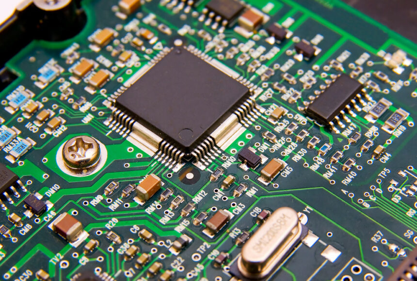
What is a PCB?
PCB design is a critical part of any electronics project. A well-designed PCB can make the difference between a successful project and a complete failure. There are many factors to consider when designing a PCB, including the layout, component placement, routing, and more. With careful planning and attention to detail, anyone can create a professional-looking PCB design.
The history of the printed circuit board.
A printed circuit board, or PCB, is a small board made of plastic that is used to connect electronic components. The first printed circuit boards were created in the early 1900s, and they have been used in a wide variety of electronic devices since then.
The first printed circuit boards were developed by the Austrian engineer Paul Eisler. Eisler invented the process of using conductive ink to print electrical patterns onto a non-conductive surface. This process was first used to create radio frequencyID tags for soldiers during World War II.
After the war, printed circuit boards began to be used in a variety of consumer electronics products, such as radios and televisions. In the 1950s, companies started mass-producing PCBs for use in these devices.
Today, PCBs are found in nearly every type of electronic device, from cell phones and computers to automobiles and appliances. They are an essential part of modern electronics and have helped make many devices smaller, lighter, and more reliable.
The design process of a PCB.
When it comes to printed circuit boards (PCBs), the design process is of the utmost importance. This is because the PCB design and development will determine how well the final product functions.
There are four main steps in the PCB design process: creating the schematic, laying out the PCB, routing the traces, and testing the board.
The first step is to create a schematic of the circuit. This can be done using a variety of software programs. Once the schematic is complete, it’s time to start laying out the PCB.
The layout of a PCB is important because it determines how everything will be arranged on the board. All of the components must be placed in their correct locations so that they can be properly soldered later on.
After all of the components have been placed on the board, it’s time to start routing traces between them. This step can be done manually or with special software programs that automatically route traces based on pre-determined rules.
Finally, once all traces have been routed, it’s time to test the board to make sure everything works as intended. This can be done by running electrical tests or by actually powering up and using the board for its intended purpose.
How to manufacture a PCB?
As the Printed Circuit Board (PCB) industry continues to grow, more and more companies are looking to get into the PCB manufacturing business. But how exactly does one go about manufacturing a PCB? In this article, we’ll take a look at the process of manufacturing a PCB, from start to finish.
The first step in manufacturing a PCB is to create the circuit design. This can be done using any number of software programs, but once the design is complete, it must be converted into a format that can be used by the PCB manufacturer. The most common format for this is Gerber files.
Once the circuit design is ready, it’s time to select the materials that will be used for the board. The two most common materials used in PCBs are FR4 and polyimide. FR4 is a type of glass-reinforced epoxy resin that is very strong and durable. Polyimide is a plastic that has a very high heat resistance and can be used in place of FR4 in some applications.
After the materials have been selected, it’s time to print out the circuit design onto a copper-clad board. This board will serve as the foundation for your PCB.
The benefits of using a PCB.

There are many benefits to using a Printed Circuit Board (PCB) over other methods of electrical wiring. PCBs are more reliable, require less maintenance, and are more compact than other methods. They also offer many safety features, such as the ability to isolate different electrical circuits from each other. This prevents shorts and reduces the risk of electrocution.
PCBs also allow for easier mass production of electronic devices. This is because the same PCB can be used for multiple devices, with only the components needing to be changed. This
significantly reduces production costs and time.
Overall, PCBs offer a number of advantages over alternative methods of electrical wiring. They are more reliable, require less maintenance, and are safer to use. Additionally, they allow for easier mass production of electronic devices, saving time and money.